Difference between revisions of "Main Page"
(→Downloads) |
|||
| Line 179: | Line 179: | ||
| − | + | [[SU717]] | |
Revision as of 13:23, 5 July 2013
Contents
Introduction
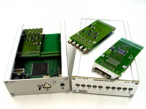
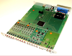
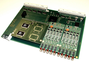
The LogicBox is an electronic data adquisition und control system based on FPGA. It was developed at the "Physikalisches Institut Universität Heidelberg" to process and control typical Nuclear Physics experiments for scientific and educational purposes only. The LogicBox consist of a FPGA main board with USB 1.1, USB-2 or VME interface and up to 8 I/O Sub-modules or extension cards with the necessary analogue or digital electronic to control or measure the desired signals. A firmware programmed into the FPGA as well as interface software allow the user to build fast and with flexibility a custom application. The system can be found in 3 different chassis:
| Format | Product id | |
|---|---|---|
| Compact | DL701 | |
| NIM | DL706 or DL709 | |
| VME | DL710 |
The provided software is implemented in LabVIEW, This software library is called "LogicPool", and content a lot of soft-modules frequently used in the Nuclear Physics. The user can interconnect these modules, as he likes to create the desired setup.
We are working to improve the system with new sub-modules/extensions boards and faster interface to be able to process more data. At this moment we have developed 30 sub-modules as multiple coincidence, fan in / fan out, splitter, logic, discriminator, ADC, TDC, etc.,
The logicBox is the ideal replacement of the typical NIM racks with several non programmable NIM modules frequently used in the Nuclear Physics, which implement trigger Logic, rate meter, Time to digital converter, acquisition, etc.
Documentation
Submodules (Extension boards)
Downloads
Firmware update (only DL706 and DL709)
Test
LogicPool (QDC)
This VHDL module needs a SU717 hardware sub-module to work.
Register Map
→ Read registers
| Register address | Name | Data |
| 0 | OUT_BUS | Bit 7..0: Bus number that this module will drive |
| 1 | ADC(W) | Bit 15..0: |
| 3 | SPI |
→ Write registers
| Register address | Register
Name |
Data |
| 0 | IN_TRIGGER | Bit 7..0: signal number to connect this module input |
| 1 | Gate(W) | Bit 15..0: gate width in 10 ns steps. |
| 2 | Control 1 | Bit 7..0: Start delay
Bit 16..14: Mode |
| 3 | SPI | |
| 4 | Control 2 | Bit 7..0: Stop Delay |
LabVIEW Vi
Gated Integrator with ADC and baseline correction.
Support: SU717
Inputs:
TRIGGER: Rising edge starts Gate for integration and data sampling.
Outputs:
BUS: Data & Strobe for ADC
PARAMS:
Gate/10ns: Length of Gate after Trigger in 10 ns
StartDelay: sampling point after start of GATE (incl. ADC-Pipeline=18)
StopDelay: sampling point after end of GATE (incl. ADC-Pipeline=18)
Mode:
normal: StopData-StartData will be recorded ( 15 bit signed!)
stop: Only StopData value recorded
start: Only StartData value recorded
start+stop: StartData & StopData values recorded
all: All ADC data values in gate recorded
Function:
Connect: connects in&outputs and loads all parameters.
Set TRIGGER: change input TRIGGER.
Get BUS: return Strobe
Write Params&Clear: loads parameters, clears FIFO
Read ADC: read data value
QDC#: number of module (must be unique)
USB In and USB Out are related to the selected USB interface!
No connection uses a global parameter, set by OPEN.vi!
LabVIEW demos
Supported hardware


